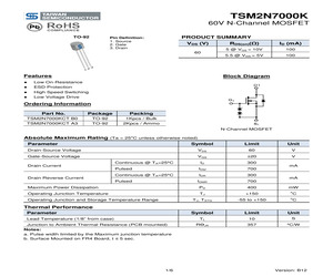
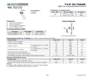
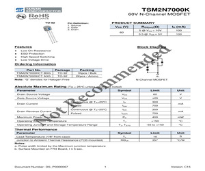
TSM2N7000K 60V N-Channel MOSFET TO-92 PRODUCT SUMMARY Pin Definition: 1. Source 2. Gate 3. Drain VDS (V) 60 Features RDS(on)() ID (mA) 5 @ VGS = 10V 100 5.5 @ VGS = 5V 100 Block Diagram Low On-Resistance ESD Protection High Speed Switching Low Voltage Drive Ordering Information Part No. Package Packing TSM2N7000KCT B0 TSM2N7000KCT A3 TO-92 TO-92 1Kpcs / Bulk 2Kpcs / Ammo N-Channel MOSFET Absolute Maximum Rating (Ta = 25oC unless otherwise noted) Parameter Symbol Limit Unit Drain-Source Voltage VDS 60 V Gate-Source Voltage VGS 20 V Continuous @ TA=25C ID 300 Pulsed IDM 700 Continuous @ TA=25C IDR 300 Pulsed IDMR 700 Maximum Power Dissipation PD 400 Operating Junction Temperature TJ +150 o TJ, TSTG -55 to +150 o Symbol Limit Unit TL 10 S RJA 357 C/W Drain Current Drain Reverse Current Operating Junction and Storage Temperature Range mA mA mW C C Thermal Performance Parameter Lead Temperature (1/8" from case) Junction to Ambient Thermal Resistance (PCB mounted) Notes: a. Pu
 6 Pages, 160 KB, Original
TSM2N7000K 60V N-Channel MOSFET TO-92 PRODUCT SUMMARY Pin Definition: 1. Source 2. Gate 3. Drain VDS (V) 60 Features Low On-Resistance ESD Protection High Speed Switching Low Voltage Drive RDS(on)() ID (mA) 5 @ VGS = 10V 100 5.5 @ VGS = 5V 100 Block Diagram Ordering Information Part No. Package Packing TSM2N7000KCT B0G TSM2N7000KCT A3G TO-92 TO-92 1Kpcs / Bulk 2Kpcs / Ammo Note: "G" denotes for Halogen Free N-Channel MOSFET Absolute Maximum Rating (Ta = 25C unless otherwise noted) Parameter Symbol Limit Unit Drain-Source Voltage VDS 60 V Gate-Source Voltage VGS 20 V Continuous @ TA=25C ID 300 Pulsed IDM 700 Continuous @ TA=25C IDR 300 Pulsed IDMR 700 Maximum Power Dissipation PD 400 mW Operating Junction Temperature TJ +150 C TJ, TSTG -55 to +150 C Symbol Limit Unit TL 10 S RJA 357 C/W Drain Current Drain Reverse Current Operating Junction and Storage Temperature Range mA mA Thermal Performance Parameter Lead Temperature (1/8" from case) Junction to Ambient Thermal Resis
 6 Pages, 180 KB, Original
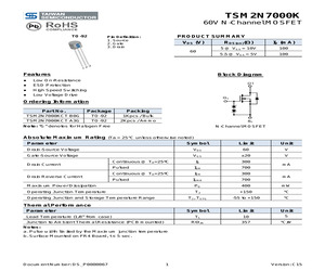
TSM2N7000K 60V N-Channel MOSFET TO-92 PRODUCT SUMMARY VDS (V) RDS(on)() Pin Definition: 1. Source 2. Gate 3. Drain 60 Features ID (mA) 5 @ VGS = 10V 100 5.5 @ VGS = 5V 100 Block Diagram Low On-Resistance ESD Protection High Speed Switching Low Voltage Drive Ordering Information Part No. Package Packing TSM2N7000KCT B0 TO-92 1Kpcs / Bulk TSM2N7000KCT A3 TO-92 2Kpcs / Ammo N-Channel MOSFET Absolute Maximum Rating (Ta = 25oC unless otherwise noted) Parameter Symbol Limit Unit Drain-Source Voltage VDS 60 V Gate-Source Voltage VGS 20 V Continuous @ TA=25C ID 300 Pulsed IDM 700 Continuous @ TA=25C IDR 300 Pulsed IDMR 700 Maximum Power Dissipation PD 400 Operating Junction Temperature TJ +150 o C TJ, TSTG -55 to +150 o C Symbol Limit Unit TL 10 S RJA 357 C/W Drain Current Drain Reverse Current Operating Junction and Storage Temperature Range mA mA mW Thermal Performance Parameter Lead Temperature (1/8" from case) Junction to Ambient Thermal Resistance (PCB mounted) Notes: a. Pu
 5 Pages, 179 KB, Original
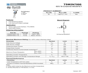
TSM2N7000 60V N-Channel MOSFET Pb) COMPLIANCE TO-92 : as 6] Pin Definition: PRODUCT SUMMARY { . u 2. Gate Vos (V) Rpsyon)(Q) Ib (mA) 3. Drain 60 5 @ Ves = 10V 75 123 Features Block Diagram e Fast Switching Speed D e Low Input and Output Leakage Application e Direct Logic-Level Interface: TTL/CMOS a o e Solid-State Relays Ordering Information Part No. Package Packing S TSM2N7000CT BO TO-92 1Kpcs / Bulk N-Channel MOSFET TSM2N7000CT A3 TO-92 2Kpcs / Ammo Absolute Maximum Rating (Ta = 25C unless otherwise noted) Parameter Symbol Limit Unit Drain-Source Voltage Vos 60 V Gate-Source Voltage Ves +20 V Continuous Drain Current Ib 200 mA Pulsed Drain Current lom 500 mA Continuous Source Current (Diode Conduction)* Is 500 mA Ta = 25C 350 Maximum Power Dissipation Pp mW Ta = 75C 280 Operating Junction Temperature Ty +150 C Operating Junction and Storage Temperature Range Ty, Tste -55 to +150 C Thermal Performance Parameter Symbol Limit Unit Lead Temperature (1/8 from case) TL 10 Ss
 5 Pages, 86 KB, Scan
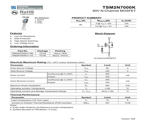
TSM2N7000K 60V N-Channel MOSFET TO-92 PRODUCT SUMMARY Pin Definition: 1. Source 2. Gate 3. Drain VDS (V) 60 Features RDS(on)() ID (mA) 5 @ VGS = 10V 100 5.5 @ VGS = 5V 100 Block Diagram Low On-Resistance ESD Protection High Speed Switching Low Voltage Drive Ordering Information Part No. Package Packing TSM2N7000KCT B0 TSM2N7000KCT A3 TO-92 TO-92 1Kpcs / Bulk 2Kpcs / Ammo N-Channel MOSFET Absolute Maximum Rating (Ta = 25oC unless otherwise noted) Parameter Symbol Limit Unit Drain-Source Voltage VDS 60 V Gate-Source Voltage VGS 20 V Continuous @ TA=25C ID 300 Pulsed IDM 700 Continuous @ TA=25C IDR 300 Pulsed IDMR 700 Maximum Power Dissipation PD 400 Operating Junction Temperature TJ +150 o TJ, TSTG -55 to +150 o Symbol Limit Unit TL 10 S RJA 357 C/W Drain Current Drain Reverse Current Operating Junction and Storage Temperature Range mA mA mW C C Thermal Performance Parameter Lead Temperature (1/8" from case) Junction to Ambient Thermal Resistance (PCB mounted) Notes: a. Pu
 7 Pages, 161 KB, Original
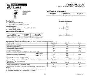
TSM2N7000 60V N-Channel MOSFET SOT-92 PRODUCT SUMMARY VDS (V) RDS(on)() Pin Definition: 1. Gate 2. Source 3. Drain 60 5 @ VGS = 10V Features ID (mA) 500 Block Diagram Fast Switching Speed Low Input and Output Leakage Application Direct Logic-Level Interface: TTL/CMOS Solid-State Relays Ordering Information Part No. Package Packing TSM2N7000CT B0 TSM2N7000CT A3 TO-92 TO-92 1Kpcs / Bulk 2Kpcs / Ammo N-Channel MOSFET Absolute Maximum Rating (Ta = 25oC unless otherwise noted) Parameter Symbol Limit Unit Drain-Source Voltage VDS 60 V Gate-Source Voltage VGS 20 V ID 200 mA IDM 500 mA IS 500 mA Continuous Drain Current Pulsed Drain Current Continuous Source Current (Diode Conduction) a,b o Maximum Power Dissipation Ta = 25 C PD o Ta = 75 C Operating Junction Temperature 280 mW +150 o TJ, TSTG -55 to +150 o Symbol Limit TL 10 TJ Operating Junction and Storage Temperature Range 350 C C Thermal Performance Parameter Lead Temperature (1/8" from case) Junction to Ambient Thermal Res
 4 Pages, 181 KB, Original
TSM2N7000K 60V N-Channel MOSFET TO-92 PRODUCT SUMMARY Pin Definition: 1. Source 2. Gate 3. Drain VDS (V) 60 Features RDS(on)() ID (mA) 5 @ VGS = 10V 100 5.5 @ VGS = 5V 100 Low On-Resistance ESD Protection High Speed Switching Low Voltage Drive Ordering Information Package Packing TSM2N7000KCT B0G TSM2N7000KCT A3G TO-92 TO-92 1Kpcs / Bulk 2Kpcs / Ammo mm Part No. en de d Block Diagram Note: "G" denotes for Halogen Free N-Channel MOSFET Parameter eco Absolute Maximum Rating (Ta = 25C unless otherwise noted) Symbol Limit Unit VDS 60 V VGS 20 V Continuous @ TA=25C ID 300 Pulsed IDM 700 Continuous @ TA=25C IDR 300 Pulsed IDMR 700 Maximum Power Dissipation PD 400 mW Operating Junction Temperature TJ +150 C TJ, TSTG -55 to +150 C Symbol Limit Unit TL 10 S RJA 357 C/W Drain-Source Voltage tR Gate-Source Voltage Drain Current No Drain Reverse Current Operating Junction and Storage Temperature Range mA mA Thermal Performance Parameter Lead Temperature (1/8" from case) Junction to
 6 Pages, 171 KB, Original
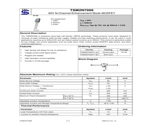
TSM2N7000 60V N-Channel Enhancement Mode MOSFET Pin assignment: 1. Gate 2. Source 3. Drain VDS = 60V ID = 200mA RDS (on), Vgs @ 10V, Ids @ 500mA = 5.0 General Description The TSM2N7000 is produced using high cell density, DMOS technology. These products have been designed to minimize on-state resistance while provide rugged, reliable and fast switching performance. It can be used in most applications requiring up to 200mA DC and can deliver pulsed currents up to 500mA. This product is particularly suited for low voltage, low current application such as small servo motor control, power MOSFET gate drivers, and other switching applications. Features Ordering Information High density cell design for low on-resistance Voltage control small signal switch Rugged and reliable High saturation current capability Provide in TO-92 package Part No. Packing Package TSM2N7000CT A3 Ammo pack TO-92 TSM2N7000CT B0 Bulk pack Block Diagram Absolute Maximum Rating (Ta = 25oC un
 3 Pages, 121 KB, Original
TSM2N7000 60V N-Channel MOSFET Pb) COMPLIANCE TO-92 : as 6] Pin Definition: PRODUCT SUMMARY { . u 2. Gate Vos (V) Rpsyon)(Q) Ib (mA) 3. Drain 60 5 @ Ves = 10V 75 123 Features Block Diagram e Fast Switching Speed D e Low Input and Output Leakage Application e Direct Logic-Level Interface: TTL/CMOS a o e Solid-State Relays Ordering Information Part No. Package Packing S TSM2N7000CT BO TO-92 1Kpcs / Bulk N-Channel MOSFET TSM2N7000CT A3 TO-92 2Kpcs / Ammo Absolute Maximum Rating (Ta = 25C unless otherwise noted) Parameter Symbol Limit Unit Drain-Source Voltage Vos 60 V Gate-Source Voltage Ves +20 V Continuous Drain Current Ib 200 mA Pulsed Drain Current lom 500 mA Continuous Source Current (Diode Conduction)* Is 500 mA Ta = 25C 350 Maximum Power Dissipation Pp mW Ta = 75C 280 Operating Junction Temperature Ty +150 C Operating Junction and Storage Temperature Range Ty, Tste -55 to +150 C Thermal Performance Parameter Symbol Limit Unit Lead Temperature (1/8 from case) TL 10 Ss
 5 Pages, 87 KB, Scan


